In this quick tutorial you will learn about the I²C communication protocol. You may have already noticed that I²C is widely used in the embedded world, to plug and read all those wonderful sensors. Let’s see why.
Introduction
I²C (pronounced I-squared-C) is a 2-wires protocol invented by Philips (today NXP Semiconductors) back in the 80’s. For a time, every silicon constructor needed to pay Philips (or NXP) a license fee to implement I²C in their designs, but since 2006 it’s not needed anymore.
I²C stands for Inter-Integrated Circuit and its main characteristics are that it only needs 2 wires, it’s bidirectional and it’s used on short distances (PCB level).
The original designs allowed communication speeds up to 100 KHz, but it went progressively incrementing up to 5 MHz (every I²C device supports a maximum I²C speed and it’s detailed in the device’s datasheet).
I²C, in the Arduino world, is sometimes referred as the “2-wire” communication interface. In fact, in order to use I²C you need to #include the file <Wire.h>. In the Linux/PC world you may know it as SMBus or SMB, that means System Management Bus, and it’s straightly derived from I²C, to be used in motherboards. The differences are minimum: it has more restrictions compared to I²C, timeout time and voltage levels are different. But in most cases both protocols are compatible.
Introduction – Design
I²C is what it’s called a bus. A bus allows connecting several devices in parallel. Every device in the bus shares the two I²C lines. These two lines are called SDA and SCL.
In the I²C bus there is at least one device that acts as master and at least one slave device. The master initiates the communication and the slave respond to the master’s requests.
Since the bus allows the interconnection of several slave devices, the I²C bus implements an addressing protocol: every slave on the bus has an unique ID. This ID (often referred as I²C address) can be 7-bit or 10-bit long. When the master initiates the communication, it sends the I²C address of the slave device it wants to talk to. Only the slave device that matches the I²C address will answer.
By moving the SDA and SCL lines, the master will send and receive data from the slave device. The master will keep track of the slave answers by the means of the ACK/NACK bit that the slave will send (more on this later), along with other data.
By using the described facilities above, the master will read and write from/to the slave device. This is how your microcontroller reads out, for example, the acceleration values from an accelerometer.
Hardware – SDA and SCL
The SDA and SCL signals are the physical layer of the I²C bus. SCL is the clock signal and SDA is the data signal. The clock signal is generated by the master, although the slave can pull it low to signal the master to wait, usually because it has data to process or needs time to elaborate a request.

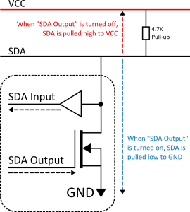
Every device in the I²C bus (masters and slaves) will be connected to the SDA and SCL lines. You may intuit that this could lead to potential hardware problems, like several devices pulling the line high and low at the same time, leading to, inevitably, “breaking something”. But for the I²C bus this is not the case because the SDA and SCL signals are open-drain.
Open-drain (without entering into too much detail) is a type of output that can only be pulled low (to ground). Doing this will generate a logic “0”. When it’s not pulled low, it is in a state called “tri-state”, or “high impedance”. In this state, the output is not being driven high nor low.
So how do we generate a logic “1”? By adding a pull-up resistor to every I²C line. When a I²C device wants to send a “0”, it pulls the line low. When it wants to send a “1”, it releases the line (into tri-state) and the pull-up resistor will take the line high.

A pull-up resistor in the I²C lines is mandatory. It’s usually a resistor of 4.7K Ohm but may vary according the the circuit and/or the requirements master and slave devices involved.
This method also ensures that no device should be able to “force” a high signal level and thus going in conflict with another device in the bus (possibly damaging it). This also allows the slave to drive the SDA line and send data back to the master (and thus making the I²C bus conveniently bi-directional).
Hardware – the pull-up resistor
The pull-up resistor topic needs some thoughts on its own, specially when connecting several breakout boards that include the pull-up resistors on-board.
Some development boards and breakout boards (from Artekit and others) sometimes include the pull-up resistor already mounted. This is done as a “feature” to allow the user to “plug-and-play” the device without the need of connecting the resistor by himself/herself. While this is handy, sometimes can lead to problems when connecting several board together (by the tenths). All those pull-up resistors will end summing up, and the results is that every device connected to the bus will need more “strength” to pull the line low. Some devices may not make it, specially those so-called low-power devices. But this case is very rare.
Another thing to take into consideration is the case when the master and the slave have different operating voltages. As seen before, the pull-up resistors of the I²C lines are usually connected between the SDA/SCL lines and the operating voltage of the device (3.3V or 5V, for example). This means that you can connect the I²C lines between devices with different operating voltages, as long as you connect the pull-ups to the lower of the two voltages. For example between a 3.3V microcontroller and a 5V DS1307 RTC, you can connect the SDA and SCL lines with a pull-up to 3.3V. This particular case (with 3.3V and 5V devices) will work OK on most cases, because a logic “1” at 3.3V should be OK for a 5V device. That is, the 5V device will “see” a logic “1” even if the voltage doesn’t reach the full 5V.
On breakout boards with the pull-up resistors already mounted, this could be a problem. For example, in our tutorial about the AK-DS1307 board connected to a Raspberry Pi, you can see that we suggest to use a logic level converter. That is because the AK-DS1307 board includes the pull-up resistors connected to VCC (5V). And as we’ve seen before, the I²C lines of the Raspberry Pi, being those open-drain, will be pulled-up to 5V, instead of 3.3V.
Here you may go deeper and understand how the input/output stage of your microcontroller is built. Some 3.3V devices allows 5V signals on some pins (sometimes referred as “5V tolerant” pins), and the problem wouldn’t exist.
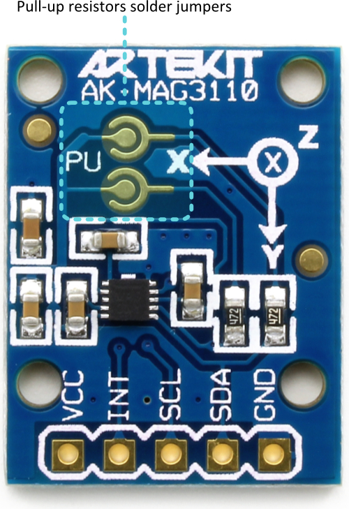
For these reasons, new Artekit board designs includes the pull-up resistors as usual, but connected through a solder jumper. If you have different voltages or the pull-ups resistors already exist somewhere in your circuit, you can choose to skip the resistors included in the board. Otherwise, put a little solder on each jumper and you are ready to go.

Protocol
The I2C protocol is not as straightforward as other protocols can be (like an UART or SPI). The protocol is about combining the SDA and SCL signals to control the flow of the communication, other than passing data between the master and the slave.
In the next illustration you can see a typical I2C transaction.

In a quick overview, what we see here is a START condition, two 8 bit bursts, two ACKs and a STOP condition.
START condition
With the START condition, the master signals the slaves that a transaction is about to start. A START condition consists in a low SDA signal while the SCL line is high.
Slave address
Following the START condition, the master sends the 7-bit address of the slave device it wants to talk to. The slave address is a combination of the 7-bit address (bits 1-7) and the LSB bit (bit 0) that determines if the current transaction is a read or a write operation. That is, if bit 0 = 0, the master is writing into the I2C slave device; if the bit 0 = 1, the master is reading from the I2C slave.
If there is a slave device that matches said address, it will answer with an ACK.
10-bit slave address
Some slave devices may implement a 10-bit slave address. In this case, the master address it by sending two bytes (instead of one) composed in the following way:
- a first byte with the form b11110XXX, where the last three bits are: the MSB of the slave address, the bit 8 of the slave address and the read/write bit (as in the 7-bit address we’ve seen before)
- a second byte with the rest of the slave address (bits 0 – 7)
The slave will answer ACK to both bytes, and then the transaction continues as usual.
ACK/NACK
The ACK/NACK is the feedback bit a master or a slave sends, and it has different meanings:
When the master is transmitting:
- the slave sends ACK when it correctly receives a byte
- the slave sends nothing (a NACK) when it’s unable to receive more data or the received byte is invalid.
When the slave is transmitting:
- the master sends ACK for every byte it receives
- the master sends NACK when it wants to end the transaction (signals the slave to stop sending data).
Clock stretching
Just before the ninth clock pulse (before the ACK/NACK) the receiving slave device has the possibility to force the SCL line low. This is called clock stretching and indicates the master device to hold until the slave device is ready to receive more data.
The master, after the eighth clock pulse, will wait until the SCL signal goes high before sending the ninth clock pulse, allowing the slave device to clock-stretch the SCL line.
Data
Depending on the value of the bit 0 of the previously transmitted slave address, a write or read operation will take place. In both cases the SCL line is controlled by the master.
For a read operation, the master controls the SCL line and the slave controls the SDA line. The master will send 9 clock pulses and the slave will shift out 8 bits of data. On the ninth clock, the master will send an ACK (or NACK). When the master is done reading from the slave, it will force a NACK and then a STOP condition.
For a write operation, the master controls both the SCL line and the SDA line. The master will send 9 clock pulses and will shift out 8 bits of data. On the ninth clock the slave will send an ACK (or NACK).
STOP condition
The transaction ends with a STOP condition. It consists in a low SCL signal followed by a high SDA signal. After this, both the master and the slave release the lines.
Repeated START condition
In a multi-master configuration, there is the possibility for the master to own the bus in order to make several transactions without being interrupted by another master. In this case is used what is called a Repeated START condition.

When doing several transactions, instead of sending a STOP and THEN a START (and thus risking that another master takes control of the bus in-between), the master can send a START without previously sending a STOP.
After this, the communication flow continues as a normal transaction by sending the slave address.
This is also a requirement for many slave devices. For example the Freescale MMA8452Q accelerometer, needs the following sequence (borrowed from the datasheet):

The master sends a START condition and then the slave address with the write-bit set. Then the register address of the MMA8452Q the master wants to read. After this the master sends a repeated START, followed by the slave address (again) but this time with the read-bit set. Then the slave sends the contents of the register.
Conclusion
This should be enough for a quick intro about I2C. To get detailed information it could be a good idea to take a look at the official I2C specifications. Make sure you also read the Wikipedia entry for I2C.
We hope you enjoyed it. Feel free to ask/correct/discuss down here in the comments or through the forum.
The Artekit Team.


